Product Overview
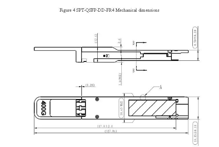
The SPT-QD04G-FR4 is a QSFP-DD packaged 400G-FR4 optical transceiver module that supports a 400Gbps data transmission rate with a maximum transmission distance of 2km over single-mode fiber (with FEC). This module features an LC duplex connector and a 4-channel CWDM wavelength multiplexing/demultiplexing design (1271/1291/1311/1331nm) with 106.25Gbps PAM4 modulation per channel and a maximum power consumption of 12W, and is suitable for data center interconnect applications.
Product Features
- QSFP-DD MSA rev5.0 compliant: Complies with the QSFP-DD Multi-Source Agreement standard
- 100G Lambda MSA compliant: Complies with the 100G Lambda MSA standard
- 802.3cu compliant: Complies with the IEEE 802.3cu standard
- 400GE FR4 specification compliant: Complies with the 400G Ethernet FR4 specification
- QSFP-DD CMIS 4.0 management interface compliant: Supports the CMIS 4.0 management interface
- 400Gbps data rate: 8×53.125Gbps PAM4 electrical interface (400GAUI-8)
- 2km transmission distance: Maximum transmission distance of 2km over single-mode fiber (with FEC)
- LC duplex connector: Standard LC duplex fiber optic connector
- 4-channel CWDM design: 4 CWDM wavelength channels with multiplexing/demultiplexing (1271/1291/1311/1331nm)
- 425Gbps aggregate bit rate: 4×106.25Gbps optical signal transmission
- Low power consumption: Maximum power consumption of 12W
- +3.3V single power supply: Simplified power supply design
- RoHS-2 compliant: Complies with RoHS-2 environmental standards
- Non-hermetic package design: Suitable for various environmental conditions
- DDM digital diagnostic monitoring: Supports I²C interface digital diagnostic management (CMIS 4.0)
Product Specifications
| Item | Specification |
|---|---|
| Product Model | SPT-QD04G-FR4 |
| Package Type | QSFP-DD |
| Data Rate | 400Gbps (8×53.125Gbps PAM4 electrical interface) |
| Optical Signal Rate | 425Gbps (4×106.25Gbps) |
| Transmission Distance | 2km (single-mode fiber, with FEC) |
| Fiber Type | Single-mode fiber |
| Interface Type | LC Duplex |
| Modulation Format | PAM4 |
| Channel Wavelength | 1271/1291/1311/1331nm (CWDM) |
| Total Average Launch Power | ≤9.5dBm |
| Average Launch Power (per channel) | -3.3 ~ 3.5dBm |
| Optical Modulation Amplitude (OMA, per channel) | -0.2 ~ 3.7dBm |
| Extinction Ratio (ER) | ≥3.5dB |
| Side Mode Suppression Ratio (SMSR) | ≥30dB |
| TDECQ (ER≥4.5dB) | ≤3.4dB |
| Launch Power (OMA minus TDECQ, ER≥4.5dB) | ≥-1.7dB |
| Launch Power (OMA minus TDECQ, ER<4.5dB) | ≥-1.6dBm |
| Launch Power Difference Between Any Two Channels (OMA) | ≤4dB |
| RIN17.1OMA | ≤-136dB/Hz |
| Optical Return Loss Tolerance | ≤17.1dB |
| Transmitter Reflectance | ≤-26dB |
| Average Launch Power OFF (per channel) | ≤-20dBm |
| Average Receive Power (per channel) | -7.3 ~ 3.5dBm |
| Receive Power (OMA, per channel) | ≤3.7dBm |
| Receive Power Difference Between Any Two Channels (OMA) | ≤4.1dB |
| Receiver Sensitivity (OMA, per channel) | See Note |
| LOS Assert | ≤-20dBm |
| LOS De-Assert | ≤-8.6dBm |
| LOS Hysteresis | 0.5dB |
| Receiver Reflectance | ≤-26dB |
| Damage Threshold (per channel) | 4.5dBm |
| SECQ (channel under test) | 0.9 ~ 3.4dB |
| OMA of Each Aggressor Channel | 1.5dBm |
| BER FLOOR | 1E-6 @ -3.1 ~ 2dBm |
| Operating Temperature | Commercial (0°C ~ 70°C) |
| Supply Voltage | +3.3V |
| Maximum Power Consumption | 12W |
Electrical Interface Characteristics
| Parameter | Min | Typ | Max | Unit |
|---|---|---|---|---|
| Signaling Rate (per channel) | 53.125±100ppm | - | - | GBd |
| Differential Input Voltage (per channel) | - | 900 | - | mV |
| Differential Output Voltage | - | - | 900 | mV |
| Transition Time | 9.5 | - | - | ps |
| Near-End Eye Width (10⁻⁶ probability) | 0.265 | - | - | UI |
| Near-End Eye Height (10⁻⁶ probability) | 70 | - | - | mV |
| Far-End Eye Width (10⁻⁶ probability) | 0.20 | - | - | UI |
| Far-End Eye Height (10⁻⁶ probability) | 30 | - | - | mV |
| Near-End Eye Linearity | 0.85 | - | - | - |
Pin Description
| Pin | Logical Symbol | Description | Mating Sequence |
|---|---|---|---|
| 1 | GND | Ground | 1B |
| 2 | CML-I Tx2n | Transmitter Inverted Data Input | 3B |
| 3 | CML-I Tx2p | Transmitter Non-Inverted Data Input | 3B |
| 4 | GND | Ground | 1B |
| 5 | CML-I Tx4n | Transmitter Inverted Data Input | 3B |
| 6 | CML-I Tx4p | Transmitter Non-Inverted Data Input | 3B |
| 7 | GND | Ground | 1B |
| 8 | LVTTL-I ModSelL | Module Select | 3B |
| 9 | LVTTL-I ResetL | Module Reset | 3B |
| 10 | VccRx | +3.3V Power Supply (Receiver) | 2B |
| 11 | LVCMOS-I/O SCL | 2-Wire Serial Interface Clock | 3B |
| 12 | LVCMOS-I/O SDA | 2-Wire Serial Interface Data | 3B |
| 13 | GND | Ground | 1B |
| 14 | CML-O Rx3p | Receiver Non-Inverted Data Output | 3B |
| 15 | CML-O Rx3n | Receiver Inverted Data Output | 3B |
| 16 | GND | Ground | 1B |
| 17 | CML-O Rx1p | Receiver Non-Inverted Data Output | 3B |
| 18 | CML-O Rx1n | Receiver Inverted Data Output | 3B |
| 19 | GND | Ground | 1B |
| 20 | GND | Ground | 1B |
| 21 | CML-O Rx2n | Receiver Inverted Data Output | 3B |
| 22 | CML-O Rx2p | Receiver Non-Inverted Data Output | 3B |
| 23 | GND | Ground | 1B |
| 24 | CML-O Rx4n | Receiver Non-Inverted Data Output | 3B |
| 25 | CML-O Rx4p | Receiver Inverted Data Output | 3B |
| 26 | GND | Ground | 1B |
| 27 | LVTTL-I ModPrsL | Module Presence | 3B |
| 28 | LVTTL-I IntL | Interrupt | 3B |
| 29 | VccTx | +3.3V Power Supply (Transmitter) | 2B |
| 30 | Vcc1 | +3.3V Power Supply | 2B |
| 31 | LVTTL-I InitMode | Initialization Mode (called LPMODE in legacy QSFP applications) | 3B |
| 32 | GND | Ground | 1B |
| 33 | CML-I Tx3p | Transmitter Non-Inverted Data Input | 3B |
| 34 | CML-I Tx3n | Transmitter Inverted Data Input | 3B |
| 35 | GND | Ground | 1B |
| 36 | CML-I Tx1p | Transmitter Non-Inverted Data Input | 3B |
| 37 | CML-I Tx1n | Transmitter Inverted Data Input | 3B |
| 38 | GND | Ground | 1B |
| 39 | GND | Ground | 1A |
| 40 | CML-I Tx6n | Transmitter Inverted Data Input | 3A |
| 41 | CML-I Tx6p | Transmitter Non-Inverted Data Input | 3A |
| 42 | GND | Ground | 1A |
| 43 | CML-I Tx8n | Transmitter Inverted Data Input | 3A |
| 44 | CML-I Tx8p | Transmitter Non-Inverted Data Input | 3A |
| 45 | GND | Ground | 1A |
| 46 | Reserved | Reserved (For Future Use) | 3A |
| 47 | VS1 | Module Vendor Specific 1 | 3A |
| 48 | VccRx1 | +3.3V Power Supply | 2A |
| 49 | VS2 | Module Vendor Specific 2 | 3A |
| 50 | VS3 | Module Vendor Specific 3 | 3A |
| 51 | GND | Ground | 1A |
| 52 | CML-O Rx7p | Receiver Non-Inverted Data Output | 3A |
| 53 | CML-O Rx7n | Receiver Inverted Data Output | 3A |
| 54 | GND | Ground | 1A |
| 55 | CML-O Rx5p | Receiver Non-Inverted Data Output | 3A |
| 56 | CML-O Rx5n | Receiver Inverted Data Output | 3A |
| 57 | GND | Ground | 1A |
| 58 | GND | Ground | 1A |
| 59 | CML-O Rx6n | Receiver Inverted Data Output | 3A |
| 60 | CML-O Rx6p | Receiver Non-Inverted Data Output | 3A |
| 61 | GND | Ground | 1A |
| 62 | CML-O Rx8n | Receiver Inverted Data Output | 3A |
| 63 | CML-O Rx8p | Receiver Non-Inverted Data Output | 3A |
| 64 | GND | Ground | 1A |
| 65 | NC | No Connect | 3A |
| 66 | Reserved | Reserved (For Future Use) | 3A |
| 67 | VccTx1 | +3.3V Power Supply | 2A |
Digital Diagnostic Monitoring Functions
The digital diagnostic management interface (DDMI) is implemented through the I²C interface in compliance with CMIS 4.0. The diagnostic management functions are implemented and the data addresses are listed in the table below:
| Performance Item | Alarm & Warning Thresholds | Alarm & Warning Monitor | Monitor Data Address |
|---|---|---|---|
| Module Temperature | Low page 9 | Page 2h (128-135) | Low page (14-15) |
| Module Voltage | Low page 9 | Page 2h (136-143) | Low page (16-17) |
| Bias Current | Page 11h (143-146) | Page 2h (184-191) | Page 11h (170-177) |
| Transmitter Optical Power | Page 11h (139-142) | Page 2h (176-183) | Page 11h (154-161) |
| Receiver Optical Power | Page 11h (149-152) | Page 2h (192-199) | Page 11h (186-193) |
ESD Design
| Parameter | Threshold | Notes |
|---|---|---|
| High-Speed Pin ESD | 1KV | Human Body Model |
| Low-Speed Pin ESD | 2KV | Human Body Model |
| Air Discharge During Operation | 15KV | - |
| Direct Contact Discharges to Enclosure | 8KV | - |
Applications
- Data center interconnects
- 400G Ethernet
- Cloud computing infrastructure
- High-performance computing networks
- Enterprise network backbone
Ordering Information
| Part Number | Product Description |
|---|---|
| SPT-QD04G-FR4 | QSFP-DD Optical Transceiver, 1271/1291/1311/1331nm (CWDM), 400G FR4, 2km, LC Interface with DDM, Commercial Temperature |
Contact Information
Email: info@sopto.com.cn
Web: http://www.sopto.com.cn
Note: For customized solutions, please contact us.