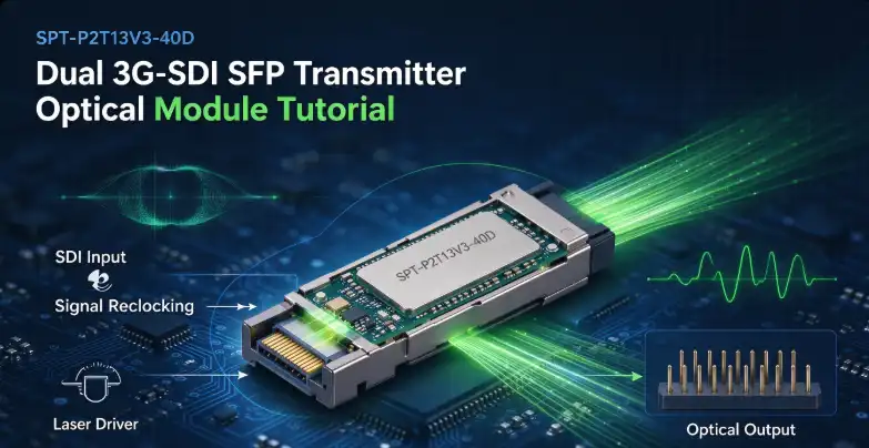
SPT-P2T13V3-40D Dual 3G-SDI SFP Transmitter Optical Module Technical Tutorial
This tutorial is written based on the Sopto SPT-P2T13V3-40D official datasheet, targeting hardware engineers and system integration engineers, covering the complete workflow of product principles, hardware wiring, power-on debugging, DDM diagnostics, and troubleshooting.
1 Product Overview
The SPT-P2T13V3-40D is a dual-transmitter SFP optical module with LC interface, 1310nm DFB laser, 40km transmission over single-mode fiber, commercial temperature range 0~70°C, compliant with SMPTE 297-2006 standard, supporting SD-SDI/HD-SDI/3G-SDI (data rates 50Mbps-2.97Gbps), full support for SDI pathological test patterns, built-in MCU control and DDM digital diagnostics, RoHS compliant, single +3.3V power supply.
Core Key Parameters (from datasheet)
| Parameter | Specification |
|---|---|
| Center Wavelength | 1260-1360nm, typical 1310nm DFB |
| Average Output Optical Power | -2 ~ +2dBm (SMF single-mode fiber output) |
| Extinction Ratio ER | >=5dB |
| SMSR Side Mode Suppression Ratio | >=30dB |
| Power Supply | 3.13-3.47V, typical 3.3V, max 500mA |
| Operating Case Temperature | 0~+70°C (commercial grade) |
| Differential Input Impedance | 90-110Ω, internal AC coupling 100Ω termination, PECL level input |
| I2C Maximum Clock | 280KHz, LVCMOS logic level |
| DDM Accuracy | Temperature ±3°C; Voltage ±3%; Bias Current ±10%; TX Optical Power ±3dB |
2 Hardware Pins and Circuit Design Guide
The module features a 20-pin SFP gold finger connector with two independent transmitter channels TX1 and TX2. The channels are completely independent and do not interfere with each other.
Key Signal Pin Descriptions
| Pin | Signal | Function Description |
|---|---|---|
| 18, 19 | TD1+ / TD1- | Channel 1 SDI differential data input, internal AC coupling, 100Ω termination, PECL differential input 400~1800mV |
| 8, 9 | TD2+ / TD2- | Channel 2 SDI differential data input |
| 20 | TX1_DIS | Channel 1 transmitter disable input, pull-up inside module; 2.0V~Vcc: laser off; 0-0.8V: transmitter on; floating = off |
| 10 | TX2_DIS | Channel 2 transmitter disable input |
| 2 | TX1_FAULT | Channel 1 fault indication (open collector output), host side must have 4.7-10K pull-up; low = normal, high = laser fault |
| 12 | TX2_FAULT | Channel 2 fault indication |
| 5 | I2C_CLK(SCL) | Management clock, host 4.7-10K pull-up to VCC_TX |
| 6 | I2C_DATA(SDA) | Management data, host 4.7-10K pull-up to VCC_TX |
| 15/16 | VCC_TX1/VCC_TX2 | Dual transmitter power supply 3.3V |
| 1/4/7/11/14/17 | VEE_TX | Module ground |
Host PCB Design Mandatory Requirements
- TX_FAULT fault pin: Open collector output, the motherboard must add a 4.7k-10kΩ pull-up resistor to 2.0V~Vcc, must not be left floating; low level 0-0.8V indicates normal operation, high level indicates laser fault.
- TX_DIS pin: Module has internal pull-up, host outputs 0-0.8V to enable laser; >2V to disable laser; floating defaults to laser disabled.
- I2C bus SCL/SDA: Motherboard must add 4.7-10K pull-up resistors, pull-up voltage uses module supply 3.3V, I2C clock rate <=280KHz, logic low 0-0.8V, high 2.0-3.3V, 0.8-2.0V is undefined region.
- SDI differential input TDx+/TDx- traces must strictly control differential impedance to 100Ω differential impedance, traces should be as short as possible, minimize vias, avoid impedance discontinuities that cause excessive jitter; the module already has internal AC coupling, do not add DC blocking capacitors on the motherboard side.
- Power supply ripple control: 3.3V power supply ripple should be less than 50mV, module maximum current 500mA, power supply circuit should have adequate ground plane.
3 Timing and Power-On Sequence
All timing references are from the original datasheet. Host software power-on logic must follow:
- Module power-on, wait for initialization time
t_init <=300ms, wait for internal MCU to complete initialization before allowing I2C read/write operations; - To enable transmitter channel: pull TX_DIS low to 0-0.8V; transmitter enable time
t_on <=1ms; - To disable transmitter channel: pull TX_DIS high > 2V, disable time
t_off <=10us; - After fault recovery: pull TX_DIS high for at least
10us(t_reset), then pull low to complete fault reset; - TX_FAULT fault reporting response time
t_fault <=100us.
4 DDM Digital Diagnostics Reading (I2C)
The module supports SFF-8472 DDM digital diagnostics.
Note: 0xA0 and 0xA2 are SFF-8472 industry standard I2C addresses, not explicitly stated in the original specification document.
- 0xA0: Read-only product ID information (model, manufacturer)
- 0xA2: DDM real-time monitoring data, reading: module temperature, supply voltage, laser bias current, TX output optical power.
Available Monitoring Items
| Monitoring Item | Measurement Range | Accuracy |
|---|---|---|
| Module Case Temperature | 0~70°C | ±3°C |
| Supply Voltage | 3.0-3.6V | ±3% |
| Laser Bias Current | 0-100mA | ±10% |
| TX Output Optical Power | -2~+2dBm | ±3dB |
5 Installation, Optical Link, and Testing Guidelines
- ESD Protection: Wear an anti-static wrist strap when inserting/removing the module. Do not touch gold fingers or optical port end faces with bare hands. This is a Class 1 laser product. Never look directly into the optical port output.
- Fiber: Must use OS2 single-mode LC duplex fiber patch cord. For 40km links, fiber loss must be calculated; module output power is -2~+2dBm, and the receive end optical power must fall within the receiver module's sensitivity window.
- Signal testing: SDI signal testing requires a video waveform monitor to test jitter specifications;
- 3G-SDI maximum allowed total jitter (pathological pattern) 120ps; HD-SDI pathological pattern 115ps; SD-SDI pathological pattern 300ps, specifications from the datasheet.
- The module supports SDI pathological pattern testing, which is an important specification for broadcast SDI modules. An SDI signal generator can be used to output pathological patterns to verify link stability.
6 Common Troubleshooting Checklist
| Fault Symptom | Troubleshooting Direction |
|---|---|
| Laser not emitting light | 1) Is TX_DIS pulled high or floating? 2) Was t_init initialization waited after power-on? 3) Is VCC supply 3.13-3.47V? 4) Check TX_Fault pin status for fault indication |
| TX_FAULT persistently high (fault) | 1) Abnormal supply voltage; 2) Internal laser fault; 3) Confirm motherboard pull-up resistor is soldered; 4) Execute TX_DIS reset procedure |
| I2C cannot be read | 1) Confirm SCL/SDA pull-up resistors; 2) I2C clock <=280KHz; 3) Wait >=300ms after power-on; 4) Check if logic levels meet LVCMOS; check if bus is stuck |
| SDI image flickering, noise | 1) Is differential input impedance 100Ω? 2) Is differential input amplitude 400-1800mV? 3) Check jitter specifications, confirm signal source output quality; 4) Excessive power supply ripple |
| DDM read data abnormal | Confirm internal/external calibration mode is used, verify read register address 0xA2, confirm I2C communication is stable |
7 Mechanical Dimensions
SFP-MSA standard package, overall dimensions 57x13.4x8.5mm; dual LC optical ports, two TOSA lateral spacing 6.25±0.05mm; gold finger is standard SFP-MSA 20-pin, physically compatible with SFP/SFP+ cages. This module is only for SDI video transmission and does not support SFP+ high-speed data protocols.
Note: If you need more customized services, please contact us.
E-mail: info@sopto.com.cn
Web: http://www.sopto.com.cn