Product Overview
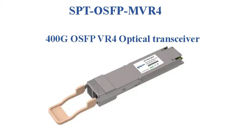
SPT-OSFP-MVR4 400G OSFP VR4 Gen2 optical transceiver is designed for use in 400G Ethernet links up to 50m over OM4/OM5 and 30m over OM3 multi-mode fiber. The module converts 4 channels of 100Gb/s (PAM4) electrical input data to 4 channels of parallel optical signals each capable of 100Gb/s operation for an aggregate data rate of 400Gb/s. On the receiver side the module converts 4 channels of parallel optical signals of 100Gb/s each channel for an aggregated data rate of 400Gb/s into 4 channels of 100Gb/s (PAM4) electrical output data. An optical fiber cable with a single MPO-12 connector can be plugged into the OSFP400 400G VR4 module receptacle. Host FEC is required to support up to OM4/OM5 50m fiber transmission.
Applications
- 400G Ethernet
- Data centers and Cloud Networks
Features
- Compliant to OSFP MSA 5.0
- Compliant with CMIS 4.0/5.0
- Parallel 4 Optical Lanes
- IEEE 802.3db 400GBASE-VR4 Specification compliant
- 4x106.25Gb/s electrical interface (400GAUI-4)
- Up to 50m over OM4/OM5 and 30m over OM3
- Maximum power consumption 9W
- MPO12-APC Receptacle
- Single +3.3V power supply
- Case temperature range: 15℃ ~ +70℃, ROHS 2.0 compliant
Absolute Maximum Ratings
| Parameter | Symbol | Min | Max | Units |
|---|---|---|---|---|
| Storage Temperature Range | TSTG | -40 | +85 | ℃ |
| Supply Voltage | VCC | -0.5 | 3.6 | V |
| Relative Humidity (non-condensing) | RH | 15% | 85% |
Operating Conditions
| Parameter | Symbol | Min | Max | Units |
|---|---|---|---|---|
| Case Temperature - Operating | TCASE | 15 | 70 | ℃ |
| Supply Voltage | VCC | 3.135 | 3.465 | V |
| Power Consumption | PDISS | 9 | W | |
| Pre-FEC Bit Error Ratio | 2.4×10⁻⁴ | |||
| Link Distance over OM3 | 0.5 | 30 | m | |
| Link Distance over OM4 | 0.5 | 50 | m |
Transmitter Optical Specifications
| Transmitter Parameter | Min | Typical | Max | Units |
|---|---|---|---|---|
| Signaling rate each lane | 53.125±100ppm | GBd | ||
| Lane Wavelength Range | 840 | 870 | nm | |
| RMS Spectral width | 0.65 | nm | ||
| Modulation Format | PAM4 | |||
| Average Optical Power per lane | -4.6 | 4 | dBm | |
| Outer Optical Modulation Amplitude (OMA outer) each lane | -2.6 | 3.5 | dBm | |
| Transmitter and Dispersion Eye Closure for PAM4 each Lane (TDECQ) | 4.4 | dB | ||
| Extinction Ratio | 2.5 | dB | ||
| Transmitter excursion each lane | 2 | dB | ||
| Transmitter transition time each lane | 17 | ps | ||
| Average Launch Power per Lane @ TX Off State | -30 | dBm | ||
| Relative Intensity Noise 12 (OMA) | -131 | dB/Hz | ||
| Optical Return Loss Tolerance | 12 | dB | ||
| Encircled Flux | ≥86% at 19um, ≤30% at 4.5um | |||
Receiver Optical Specifications
| Receiver Parameter | Min | Typical | Max | Units |
|---|---|---|---|---|
| Signaling rate each lane | 53.125±100ppm | GBd | ||
| Lane Wavelength Range | 850 | 920 | nm | |
| Modulation Format | PAM4 | |||
| Damage Threshold | 5 | dBm | ||
| Average Receive Power each lane | -6.3 | 4 | dBm | |
| Receiver Power each lane (OMA) | 3.5 | dBm | ||
| Receiver Sensitivity each lane (OMA outer) | -4.4 (for TDECQ≤1.8dB) -6.2+TDECQ (for 1.8 |
dBm | ||
| Receiver reflectance | -12 | dB | ||
| Stressed Receiver Sensitivity (OMA outer) each lane | -1.8 | dBm | ||
Stressed Conditions for Stress Receiver Sensitivity
| Parameter | Min | Typical | Max | Units |
|---|---|---|---|---|
| Stressed Eye Closure for PAM4 (SECQ) Lane under Test | 4.4 | dB | ||
| OMA outer of each Aggressor Lane | 3.5 | dBm |
Receiver Thresholds for Loss of Signal (LOS)
| Parameter | Min | Typical | Max | Units |
|---|---|---|---|---|
| RX_LOS Assert Min/Max | -15.0 | dBm | ||
| RX_LOS De-Assert Min/Max | -8.9 | dBm | ||
| RX_LOS Hysteresis | 1.5 | dB |
Digital Diagnostic Monitoring Specifications
| Parameters | Unit | Specification |
|---|---|---|
| Temperature Monitor absolute error | ℃ | ±3 |
| Supply Voltage Monitor absolute error | % | ±5 |
| Ibias Monitor absolute error | % | ±10 |
| Received Power (Rx) Monitor absolute error | dB | ±3.0 |
| Transmit Power (Tx) Monitor absolute error | dB | ±3.0 |
Low Speed Electrical Signal
| Parameter | Symbol | Min | Max | Units | Condition |
|---|---|---|---|---|---|
| VOL | 0 | 0.4 | V | IOL(max)=3.0mA for fast SCL and SDA | |
| VOH | Vcc-0.5 | Vcc+0.3 | V | 20mA for Fast-mode plus | |
| VIL | -0.3 | Vcc*0.3 | V | SCL and SDA | |
| VIH | Vcc*0.7 | Vcc+0.5 | V | SCL and SDA | |
| Capacitance for SCL and SDA I/O pin | Ci | 14 | pF | ||
| Total bus capacitive load for SCL and SDA | Cb | 100 | pF | 3.0k Ohms Pull up resistor max | |
| 200 | pF | 1.6k Ohms Pull up resistor max |
High Speed Electrical Signal
Receiver Electrical Output Characteristics at TP4
| Parameter | Min | Typical | Max | Units |
|---|---|---|---|---|
| Signaling rate per lane | 53.125 | GBd | ||
| AC common-mode output voltage (RMS) | 17.5 | mV | ||
| Differential peak-to-peak output voltage | 900 | mV | ||
| Near-end Eye height differential | 24 | mV | ||
| Near-end vertical eye closure | 7.5 | dB | ||
| Far-end Eye height differential | 24 | mV | ||
| Far-end vertical eye closure | 7.5 | dB | ||
| Common mode to differential conversion return loss | 802.3ck 120G-1 | |||
| Effective return loss | 8.5 | dB | ||
| Differential termination mismatch | 10 | % | ||
| Transition time (min 20% to 80%) | 8.5 | ps | ||
| DC common mode voltage | -350 | 2850 | mV | |
Transmitter Electrical Input Characteristics at TP1
| Parameter | Min | Typical | Max | Units |
|---|---|---|---|---|
| Signaling rate per lane | 53.125 | GBd | ||
| Differential pk-pk input voltage tolerance | 900 | mV | ||
| Common-mode to differential return loss | 802.3ck Equation (120G-1) | |||
| Effective return loss | 8.5 | dB | ||
| Differential termination mismatch | 10 | % | ||
| Module stressed input test | See 120G.3.4.1 | |||
| Single-ended voltage tolerance range | -0.4 | 3.3 | V | |
| DC common-mode voltage | -350 | 2850 | mV | |
Module Block Diagram
Figure 1: Module Block Diagram - OSFP400 400G VR4
Figure 2: OSFP400 400G contact assignment
Note: For OSFP400 400G VR4 end, only CH1~CH4 available. CH5~CH8 not connect, TX5~8p/n RX5~8p/n not connect.
Module Contact Definition
| Pin# | Symbol | Description | Logic | Direction | Plug Sequence | Notes |
|---|---|---|---|---|---|---|
| 1 | GND | Ground | 1 | |||
| 2 | TX2p | Transmitter Data Non-Inverted | CML-I | Input from Host | 3 | |
| 3 | TX2n | Transmitter Data Inverted | CML-I | Input from Host | 3 | |
| 4 | GND | Ground | 1 | |||
| 5 | TX4p | Transmitter Data Non-Inverted | CML-I | Input from Host | 3 | |
| 6 | TX4n | Transmitter Data Inverted | CML-I | Input from Host | 3 | |
| 7 | GND | Ground | 1 | |||
| 8 | TX6p | Transmitter Data Non-Inverted | CML-I | Input from Host | 3 | |
| 9 | TX6n | Transmitter Data Inverted | CML-I | Input from Host | 3 | |
| 10 | GND | Ground | 1 | |||
| 11 | TX8p | Transmitter Data Non-Inverted | CML-I | Input from Host | 3 | |
| 12 | TX8n | Transmitter Data Inverted | CML-I | Input from Host | 3 | |
| 13 | GND | Ground | 1 | |||
| 14 | SCL | 2-wire Serial interface clock | LVCMOS/I/O | Bi-directional | 3 | Open-Drain with pull-up resistor on Host |
| 15 | VCC | +3.3V Power | Power from Host | 2 | ||
| 16 | VCC | +3.3V Power | Power from Host | 2 | ||
| 17 | LPNn/PRSn | Low-Power Mode / Module Present | Multi-Level | Bi-directional | 3 | See pin description for required circuit |
| 18 | GND | Ground | 1 | |||
| 19 | RX7n | Receiver Data Inverted | CML-O | Output to Host | 3 | |
| 20 | RX7p | Receiver Data Non-Inverted | CML-O | Output to Host | 3 | |
| 21 | GND | Ground | 1 | |||
| 22 | RX5n | Receiver Data Inverted | CML-O | Output to Host | 3 | |
| 23 | RX5p | Receiver Data Non-Inverted | CML-O | Output to Host | 3 | |
| 24 | GND | Ground | 1 | |||
| 25 | RX3n | Receiver Data Inverted | CML-O | Output to Host | 3 | |
| 26 | RX3p | Receiver Data Non-Inverted | CML-O | Output to Host | 3 | |
| 27 | GND | Ground | 1 | |||
| 28 | RX1n | Receiver Data Inverted | CML-O | Output to Host | 3 | |
| 29 | RX1p | Receiver Data Non-Inverted | CML-O | Output to Host | 3 | |
| 30 | GND | Ground | 1 | |||
| 31 | GND | Ground | 1 | |||
| 32 | RX2p | Receiver Data Non-Inverted | CML-O | Output to Host | 3 | |
| 33 | RX2n | Receiver Data Inverted | CML-O | Output to Host | 3 | |
| 34 | GND | Ground | 1 | |||
| 35 | RX4p | Receiver Data Non-Inverted | CML-O | Output to Host | 3 | |
| 36 | RX4n | Receiver Data Inverted | CML-O | Output to Host | 3 | |
| 37 | GND | Ground | 1 | |||
| 38 | RX6p | Receiver Data Non-Inverted | CML-O | Output to Host | 3 | |
| 39 | RX6n | Receiver Data Inverted | CML-O | Output to Host | 3 | |
| 40 | GND | Ground | 1 | |||
| 41 | RX8p | Receiver Data Non-Inverted | CML-O | Output to Host | 3 | |
| 42 | RX8n | Receiver Data Inverted | CML-O | Output to Host | 3 | |
| 43 | GND | Ground | 1 | |||
| 44 | INT/RSTn | Module Interrupt / Module Reset | Multi-Level | Bi-directional | 3 | See pin description for required circuit |
| 45 | VCC | +3.3V Power | Power from Host | 2 | ||
| 46 | VCC | +3.3V Power | Power from Host | 2 | ||
| 47 | SDA | 2-wire Serial interface data | LVCMOS/I/O | Bi-directional | 3 | Open-Drain with pull-up resistor on Host |
| 48 | GND | Ground | 1 | |||
| 49 | TX7n | Transmitter Data Inverted | CML-I | Input from Host | 3 | |
| 50 | TX7p | Transmitter Data Non-Inverted | CML-I | Input from Host | 3 | |
| 51 | GND | Ground | 1 | |||
| 52 | TX5n | Transmitter Data Inverted | CML-I | Input from Host | 3 | |
| 53 | TX5p | Transmitter Data Non-Inverted | CML-I | Input from Host | 3 | |
| 54 | GND | Ground | 1 | |||
| 55 | TX3n | Transmitter Data Inverted | CML-I | Input from Host | 3 | |
| 56 | TX3p | Transmitter Data Non-Inverted | CML-I | Input from Host | 3 | |
| 57 | GND | Ground | 1 | |||
| 58 | TX1n | Transmitter Data Inverted | CML-I | Input from Host | 3 | |
| 59 | TX1p | Transmitter Data Non-Inverted | CML-I | Input from Host | 3 | |
| 60 | GND | Ground | 1 |
Optical Interface
The MPO-12 connectors for OSFP400 400G VR4.
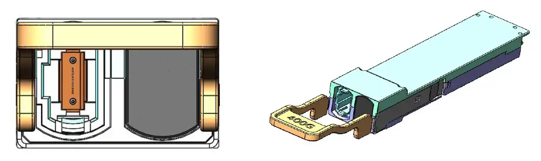
Figure 3: Optical lane assignments
Mechanical Specifications
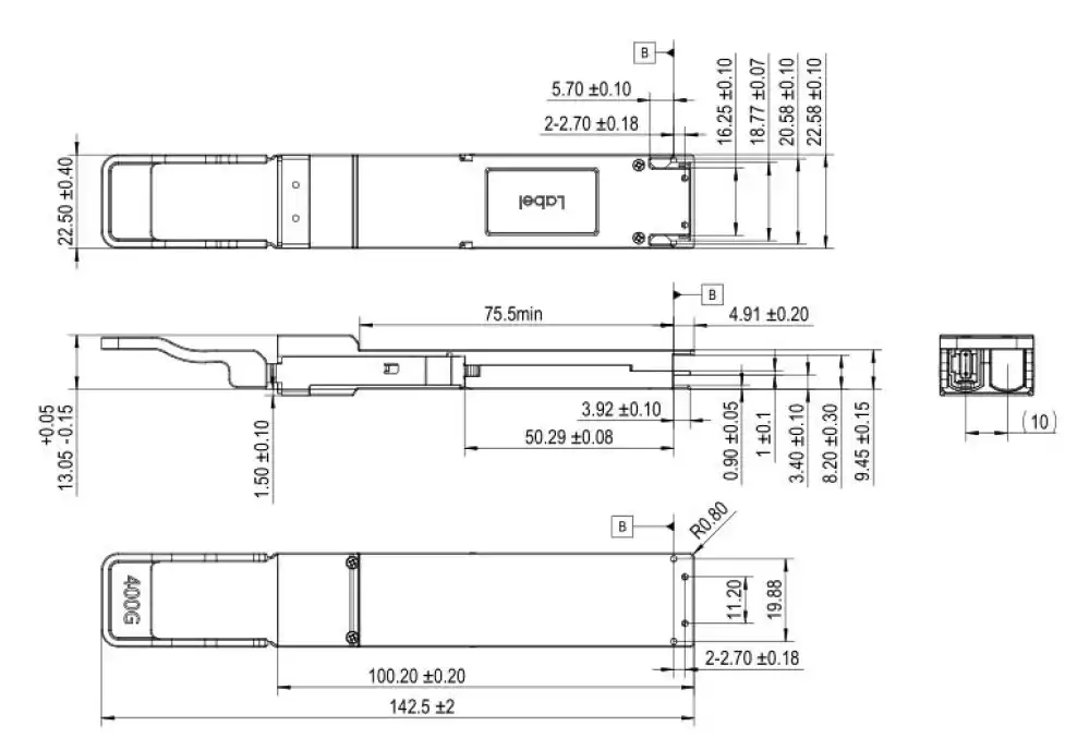
Figure 4: Mechanical Dimensions
Ordering Information
| Part Number | Description |
|---|---|
| SPT-OSFP-MVR4 | 400G OSFP VR4 Gen2 Optical transceiver |
Contact Us
Note: If you need more customized services, please contact us.
E-mail: info@sopto.com.cn
Web: http://www.sopto.com.cn