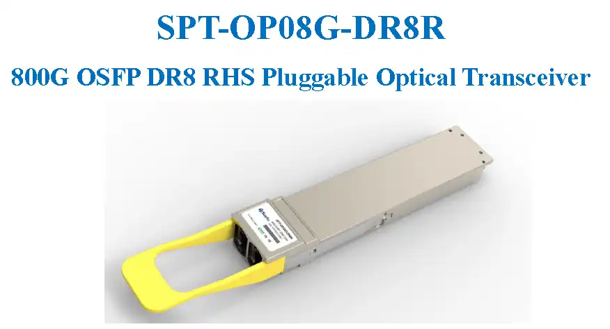
SPT-OP08G-DR8R 800G OSFP DR8 RHS Pluggable Optical Transceiver
Features
- OSFP MSA 5.0 and CMIS 5.1 compliant
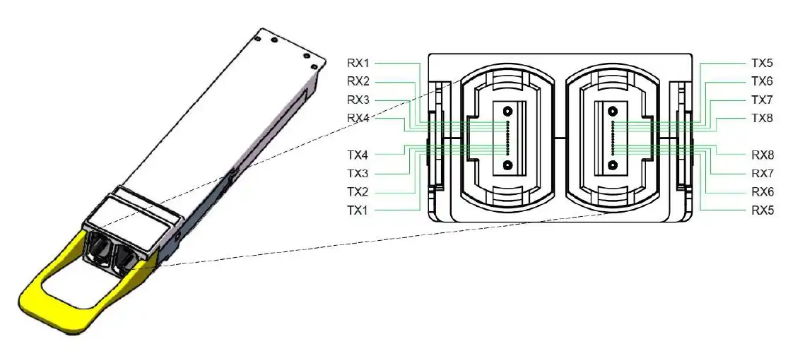
- Dual MPO-12/APC optical connectors
- 8x106.25Gbps (53.125GBd PAM4) electrical interface
- 8x106.25Gbps (53.125GBd PAM4) optical interface
- Up to 500m over SMF
- Power dissipation ≤ 16.5W
- Operating case temperature: 0°C to 70°C
- IEEE 802.3ck and IEEE 802.3df compliant
- Built-in digital diagnostic functions
- 3.3V power supply voltage
- RoHS compliant
Applications
- 800G Ethernet
- Data center networks
- InfiniBand NDR
Description
The SPT-OP08G-DR8R transceiver is designed for 800G Ethernet and InfiniBand communication application links over 500m of single-mode fiber (SMF) and it is compliant with OSFP MSA 800G Pluggable MSA CMIS 5.1, IEEE 802.3ck and IEEE 802.3df standards. The optical signal is transmitted over eight parallel channels at a central wavelength of 1310nm. The module contains 8 parallel channels on the transmitter and receiver each operating at 106.25Gbps. It is suitable for 800G Ethernet Data Center InfiniBand Breakout 2x400G DR4 or 8x100G DR Application. The optical interface is dual MPO-12/APC connector.
Absolute Maximum Ratings
| Parameter | Symbol | Min | Typ | Max | Unit |
|---|---|---|---|---|---|
| Supply Voltage | Vcc | -0.5 | - | 3.6 | V |
| Storage Temperature | Tsto | -40 | 85 | °C | |
| Relative Humidity (Non-condensing) | RH | 5 | 95 | % | |
| Control Input Voltage | Vi | -0.3 | Vcc+0.5 |
Specified Operating Conditions
| Parameter | Symbol | Min | Typ | Max | Unit |
|---|---|---|---|---|---|
| Power Supply Voltage | Vcc | 3.135 | 3.3 | 3.465 | V |
| Power Supply Current | Icc | 5271 | mA | ||
| Power Dissipation | 16.5 | W | |||
| Case Operating Temperature | Top | 0 | - | 70 | °C |
| Relative Humidity (Non-condensing) | RH | 15 | 85 | % | |
| I2C Clock Frequency | 100 | 400 | kHz |
Electrical Characteristics
| Parameter | Symbol | Min | Typ | Max | Unit |
|---|---|---|---|---|---|
| Power On Initialization Time | Tinit | 2000 | ms | ||
| Transmitter | |||||
| Signaling Speed each lane | 53.125 | GBd | |||
| Signaling Speed Tolerance | -100 | +100 | ppm | ||
| Differential pk-pk input voltage tolerance | Vinpp | 750 | mV | ||
| AC common-mode RMS voltage tolerance | 25 | mV | |||
| Differential Input Impedance | Zin | 90 | 100 | 110 | Ohms |
| Effective return loss | ERL | 8.5 | dB | ||
| Single-ended voltage tolerance range | -0.4 | 3.3 | V | ||
| DC Common Mode Voltage | -0.35 | 2.85 | V | ||
| Receiver | |||||
| Signaling Speed each lane | 53.125 | GBd | |||
| Signaling Speed Tolerance | -100 | +100 | ppm | ||
| Differential pk-pk output voltage Short mode | Voutpp | 600 | mV | ||
| Differential pk-pk output voltage Long mode | 845 | ||||
| Eye Height | EH | 15 | mV | ||
| Differential Output Impedance | Zout | 90 | 100 | 110 | Ohms |
| Transition Time 20% to 80% | TrTf | 8.5 | ps | ||
| DC Common Mode Voltage | -0.35 | 2.85 | V | ||
| AC Common Mode output Voltage (RMS) | 25 | mV | |||
Optical Characteristics
| Parameter | Symbol | Min | Typ | Max | Unit | Notes |
|---|---|---|---|---|---|---|
| Transmitter | ||||||
| Signaling Speed | 53.125 | GBd | 1 | |||
| Signaling Speed Tolerance | -100 | +100 | ppm | |||
| Modulation Format | PAM4 | |||||
| Lane Wavelength | 1304.5 | 1311 | 1317.5 | nm | ||
| Side Mode Suppression Ratio | SMSR | 30 | dB | |||
| Average TX Power | Pavg | -2.9 | 4 | dBm | 1 | |
| Outer Optical Modulation Amplitude for TDECQ<1.4dB | OMAouter | -0.8 | 4.2 | dBm | 1 | |
| Outer Optical Modulation Amplitude for 1.4dB≤TDECQ≤3.4dB | -2.2+TDECQ | |||||
| Extinction Ratio | ER | 3.5 | dB | 1 | ||
| Avg Launch Power TX Off | Poff | -15 | dBm | 1 | ||
| Transmitter and dispersion eye closure for PAM4 | TDECQ | 3.4 | dB | 1 | ||
| Transmitter eye closure for PAM4 | TECQ | 3.4 | dB | |||
| |TDECQ-TECQ| | 2.5 | dB | ||||
| Transmitter transition time | 17 | ps | ||||
| Relative Intensity Noise | RIN | -136 | dB/Hz | |||
| Optical Return Loss | ORTL | 21.4 | dB | |||
| Reflectance | -26 | dB | ||||
| Receiver | ||||||
| Signaling Speed | 53.125 | GBd | 1 | |||
| Signaling Speed Tolerance | -100 | +100 | ppm | |||
| Modulation Format | PAM4 | |||||
| Lane Wavelength | 1304.5 | 1311 | 1317.5 | nm | ||
| Damage Threshold | 5 | dBm | 1 | |||
| Average RX Power | -5.9 | 4 | dBm | 1 | ||
| RX Power (OMAouter) | 4.2 | dBm | 1 | |||
| RX Reflectance | -26 | dBm | ||||
| RX Sensitivity (OMAouter) for TECQ<1.4dB | -3.9 | dBm | 2 | |||
| RX Sensitivity (OMAouter) for 1.4dB≤TECQ≤3.4dB | -5.3+TECQ | |||||
| Stressed RX Sensitivity (OMAouter) | -1.9 | dBm | ||||
| Conditions of Stressed RX Sensitivity Test | ||||||
| Stressed Eye Closure lane under test | SECQ | 3.4 | dB | |||
| OMAouter of Each Aggressor Lane | 4.2 | |||||
Notes:
- Each lane.
- Measured with compliance test signal at TP3 for BER=2.4x10⁻⁴.
Electrical Input/Output
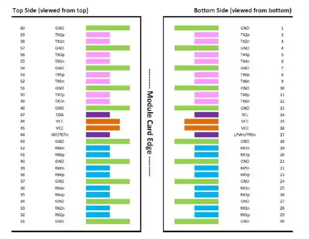
OSFP Module Contact Pad Electrical Definition
| PIN | Symbol | Logic | Description | Notes |
|---|---|---|---|---|
| 1 | GND | Ground | ||
| 2 | TX2p | CML-I | Transmitter Data Non-Inverted | |
| 3 | TX2n | CML-I | Transmitter Data Inverted | |
| 4 | GND | Ground | ||
| 5 | TX4p | CML-I | Transmitter Data Non-Inverted | |
| 6 | TX4n | CML-I | Transmitter Data Inverted | |
| 7 | GND | Ground | ||
| 8 | TX6p | CML-I | Transmitter Data Non-Inverted | |
| 9 | TX6n | CML-I | Transmitter Data Inverted | |
| 10 | GND | Ground | ||
| 11 | TX8p | CML-I | Transmitter Data Non-Inverted | |
| 12 | TX8n | CML-I | Transmitter Data Inverted | |
| 13 | GND | Ground | ||
| 14 | SCL | LVCMOS-I/O | 2-wire Serial interface clock | Open-Drain with pull up resistor on Host |
| 15 | VCC | Power from Host | +3.3V Power | |
| 16 | VCC | Power from Host | +3.3V Power | |
| 17 | LPWn/PRSn | Multi-Level | Low-Power Mode/Module Present | See pin description for required circuit |
| 18 | GND | Ground | ||
| 19 | RX7n | CML-O | Receiver Data Inverted | |
| 20 | RX7p | CML-O | Receiver Data Non-Inverted | |
| 21 | GND | Ground | ||
| 22 | RX5n | CML-O | Receiver Data Inverted | |
| 23 | RX5p | CML-O | Receiver Data Non-Inverted | |
| 24 | GND | Ground | ||
| 25 | RX3n | CML-O | Receiver Data Inverted | |
| 26 | RX3p | CML-O | Receiver Data Non-Inverted | |
| 27 | GND | Ground | ||
| 28 | RX1n | CML-O | Receiver Data Inverted | |
| 29 | RX1p | CML-O | Receiver Data Non-Inverted | |
| 30 | GND | Ground | ||
| 31 | GND | Ground | ||
| 32 | RX2p | CML-O | Receiver Data Non-Inverted | |
| 33 | RX2n | CML-O | Receiver Data Inverted | |
| 34 | GND | Ground | ||
| 35 | RX4p | CML-O | Receiver Data Non-Inverted | |
| 36 | RX4n | CML-O | Receiver Data Inverted | |
| 37 | GND | Ground | ||
| 38 | RX6p | CML-O | Receiver Data Non-Inverted | |
| 39 | RX6n | CML-O | Receiver Data Inverted | |
| 40 | GND | Ground | ||
| 41 | RX8p | CML-O | Receiver Data Non-Inverted | |
| 42 | RX8n | CML-O | Receiver Data Inverted | |
| 43 | GND | Ground | ||
| 44 | INT/RSTn | Multi-Level | Module Interrupt/Module Reset | See pin description for required circuit |
| 45 | VCC | Power from Host | +3.3V Power | |
| 46 | VCC | Power from Host | +3.3V Power | |
| 47 | SDA | LVCMOS-I/O | 2-wire Serial interface data | Open-Drain with pull up resistor on Host |
| 48 | GND | Ground | ||
| 49 | TX7n | CML-I | Transmitter Data Inverted | |
| 50 | TX7p | CML-I | Transmitter Data Non-Inverted | |
| 51 | GND | Ground | ||
| 52 | TX5n | CML-I | Transmitter Data Inverted | |
| 53 | TX5p | CML-I | Transmitter Data Non-Inverted | |
| 54 | GND | Ground | ||
| 55 | TX3n | CML-I | Transmitter Data Inverted | |
| 56 | TX3p | CML-I | Transmitter Data Non-Inverted | |
| 57 | GND | Ground | ||
| 58 | TX1n | CML-I | Transmitter Data Inverted | |
| 59 | TX1p | CML-I | Transmitter Data Non-Inverted | |
| 60 | GND | Ground |
Mechanical Specifications
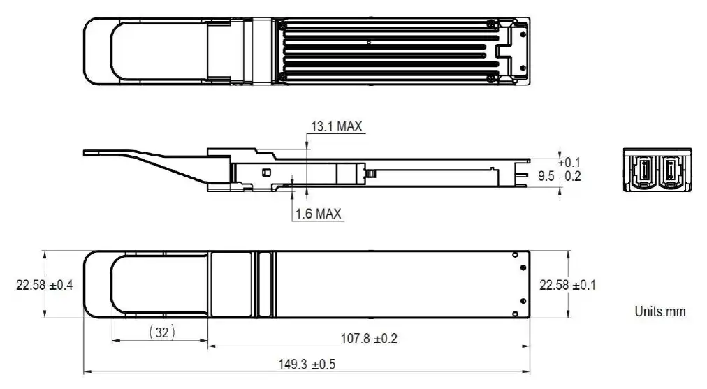
Product shall be of design, construction and physical dimensions specified on the applicable product drawing.
Optical Interface
Laser Safety
This is a Class 1 Laser Product as defined by IEC 60825-1:2014. When operated within the limits of this specification it is considered non-hazardous. Operating this product in a manner inconsistent with specifications and intended usage may result in hazardous radiation exposure.
Regulatory Certifications
This product is certified to the following regulatory standards:
| Category | Standard |
|---|---|
| Radiated Emissions | EMC Directive 2014/30/EU EN55032 CISPR32 FCC rules 47CFR Part15 ICES-003 VCCI-CISPR32 AS/NZS CISPR32 |
| Radiated Immunity | EMC Directive 2014/30/EU EN55035 CISPR35 IEC/EN61000-4-3 |
| RoHS | EU RoHS (2011/65/EU & (EU)2015/863) & UK RoHS EN IEC 63000:2018 & BS EN IEC 63000:2018 |
| Flammability (PCB) | UL Class 94V-0 |
Ordering Information
| Part Number | Product Description |
|---|---|
| SPT-OP08G-DR8R | Transceiver OSFP 800G DR8R HS 8x100G PAM4 1310nm 500m Dual MPO-12/APC SMF with DDM Commercial Temperature |
Note: If you need more customized services please contact us.
Contact Us
E-mail: info@sopto.com.cn
Web: http://www.sopto.com.cn