Product Overview
The SPT-GT4321-SB2BD is a GPON OLT SFP optical transceiver module that supports GPON/EPON/BPON protocol. The module uses Tx1490nm/Rx1310nm wavelength, supports 2.5Gbps downstream rate and 1.25Gbps upstream rate, uses SC interface, and supports DDM digital diagnostic monitoring function. Suitable for FTTH fiber to the home network, PON network and other application scenarios.
Product Features
- Supports GPON/EPON/BPON protocol
- Tx1490nm/Rx1310nm wavelength
- 2.5Gbps downstream rate/1.25Gbps upstream rate
- SC interface
- Supports DDM digital diagnostic monitoring
- Commercial temperature range: 0°C ~ +70°C
- Supports Class B+/C+/C++/C+++/C++++ optical budget levels
- Complies with SFP Multi-Source Agreement standard
- Supports hot-plugging
Absolute Maximum Ratings
| Parameter | Symbol | Min | Max | Unit |
|---|
| Supply Voltage | Vcc | -0.3 | 3.6 | V |
| Operating Temperature | TOP | 0 | 70 | °C |
| Storage Temperature | TSTG | -40 | 85 | °C |
Recommended Operating Conditions
| Parameter | Symbol | Min | Typ | Max | Unit |
|---|
| Supply Voltage | Vcc | 3.135 | 3.3 | 3.465 | V |
| Operating Temperature | TOP | 0 | - | 70 | °C |
Electrical Characteristics
| Parameter | Symbol | Min | Typ | Max | Unit |
|---|
| Supply Current | Icc | - | - | 300 | mA |
| Differential Output Voltage | VOUT | 300 | - | - | mVpp |
| Differential Output DC Common Mode Voltage | VCM | - | - | Vcc | V |
| Differential Input Voltage | VIN | 100 | - | 1600 | mVpp |
Optical Parameters - Transmitter
| Parameter | Symbol | Min | Typ | Max | Unit |
|---|
| Center Wavelength | λc | - | 1490 | - | nm |
| Spectral Width (RMS) | σ | - | - | 1 | nm |
| Average Output Power | Pout | See optical budget table | - | See optical budget table | dBm |
| Extinction Ratio | ER | 8 | - | - | dB |
| Optical Modulation Amplitude (OMA) | OMA | See optical budget table | - | - | dBm |
Optical Parameters - Receiver
| Parameter | Symbol | Min | Typ | Max | Unit |
|---|
| Center Wavelength | λc | - | 1310 | - | nm |
| Receiver Sensitivity | RXSEN | See optical budget table | - | - | dBm |
| Overload | OVERLOAD | See optical budget table | - | - | dBm |
| Return Loss | - | 12 | - | - | dB |
Optical Budget Classes
| Class | Min Avg Tx Power(dBm) | Max Avg Tx Power(dBm) | Receiver Sensitivity(dBm) | Overload(dBm) |
|---|
| Class B+ | -1 | +4 | -28 | -8 |
| Class C+ | +2 | +7 | -32 | -8 |
| Class C++ | +4 | +8 | -33 | -8 |
| Class C+++ | +5 | +9 | -34 | -8 |
| Class C++++ | +6 | +10 | -35 | -8 |
DDM Digital Diagnostic Monitoring
Alarm and Warning Thresholds
| Parameter | Temp(℃) | Voltage(V) | Bias(mA) | TX Power(dBm) | RX Power(dBm) |
|---|
| High Alarm | 100 | 3.6 | 90 | +5 ~ +8 | -8 ~ -10 |
| Low Alarm | -10 | 3 | 0 | +1.5 ~ +4 | -28 ~ -30 |
| High Warning | 95 | 3.5 | 70 | +4.5 ~ +7.5 | -9 ~ -11 |
| Low Warning | 0 | 3.1 | 0 | +2 ~ +5 | -27 ~ -29 |
Digital Diagnostic Monitor Accuracy
| Parameter | Unit | Accuracy | Range | Calibration |
|---|
| Tx Optical Power | dB | ±3 | Po: -Pomin~Pomax dBm | External/Internal |
| Rx Optical Power | dB | ±3 | Pi: Ps~Pr dBm | External/Internal |
| Bias Current | % | ±10 | Id: 1-100mA | External/Internal |
| Power Supply Voltage | % | ±3 | Recommended operating conditions | External/Internal |
| Internal Temperature | ℃ | ±3 | Recommended operating conditions | External/Internal |
Pin Definitions
| Pin | Name | Description | Type | Note |
|---|
| 1 | VeeT | Transmitter Ground | 1 | Note 5 |
| 2 | Tx Fault | Transmitter Fault Indication | 3 | Note 1 |
| 3 | Tx Disable | Transmitter Disable | 3 | Note 2 |
| 4 | MOD-DEF2 | Module Definition 2 | 3 | Note 3 |
| 5 | MOD-DEF1 | Module Definition 1 | 3 | Note 3 |
| 6 | MOD-DEF0 | Module Definition 0 | 3 | Note 3 |
| 7 | Reset | Reset signal input | 3 | - |
| 8 | BPD | Burst Power Detect (active HIGH) | 3 | Note 4 |
| 9 | RSSI-Trigger | Receiver Signal Strength Indication | 1 | - |
| 10 | VeeR | Receiver Ground | 1 | Note 5 |
| 11 | VeeR | Receiver Ground | 1 | Note 5 |
| 12 | RD- | Inv. Receiver Data Out | 3 | Note 6 |
| 13 | RD+ | Receiver Data Out | 3 | Note 6 |
| 14 | VeeR | Receiver Ground | 1 | Note 5 |
| 15 | VccR | Receiver Power Supply | 2 | Note 7 3.3V±5% |
Notes
- Note 1: TX Fault is an open collector/drain output which should be pulled up with a 4.7K–10KΩ resistor on the host board. Pull up voltage between 2.0V and VccT R+0.3V. When high output indicates a laser fault of some kind. Low indicates normal operation. In the low state the output will be pulled to < 0.8V.
- Note 2: TX disable is an input that is used to shut down the transmitter optical output. It is pulled up within the module with a 4.7–10 KΩ resistor. Its states are: Low (0 – 0.8V): Transmitter on; (>0.8 < 2.0V): Undefined; High (2.0 – 3.465V): Transmitter Disabled; Open: Transmitter Disabled.
- Note 3: Mod-Def 0, 1, 2. These are the module definition pins. They should be pulled up with a 4.7K – 10KΩ resistor on the host board. The pull-up voltage shall be VccT or VccR. Mod-Def 0 is grounded by the module to indicate that the module is present; Mod-Def 1 is the clock line of two wire serial interface for serial ID; Mod-Def 2 is the data line of two wire serial interface for serial ID.
- Note 4: BPD is pulled up internally with a 4.7K – 10KΩ resistor. Pull up voltage between 2.0V and VccT R+0.3V. When LOW this output indicates the received optical power is below the worst-case receiver sensitivity (as defined by the standard in use). HIGH indicates normal operation. In the low state the output will be pulled to < 0.8V.
- Note 5: VeeR and VeeT may be internally connected within the SFP module.
- Note 6: RD-/+ are the differential receiver outputs. They are DC coupled 100Ω differential lines which should be terminated with 100Ω (differential) at the user SERDES.
- Note 7: VccR and VccT are the receiver and transmitter power supplies. They are defined as 3.3V. Board power supply filtering should be used. When the recommended supply filtering network is used hot plugging of the SFP transceiver module will result in an inrush current of no more than 30 mA greater than the steady state value. VccR and VccT may be internally connected within the SFP transceiver module.
- Note 8: TD-/+ are the differential transmitter inputs. They are AC-coupled differential lines with 100Ω differential termination inside the module. The AC coupling is done inside the module and is thus not required on the host board.
GPON System Timing Parameters
| Parameter | Symbol | Min | Typ | Max | Unit |
|---|
| Packet Length | - | - | 600 | - | ns |
| Trigger Delay | BOPCS | - | 100 | - | ns |
| RSSI Trigger and Sample Time | Holding Time | - | 400 | - | ns |
| Internal Delay | Conversion Time | - | 500 | - | μs |
Recommended Interface Circuit
Please refer to the recommended interface circuit diagram
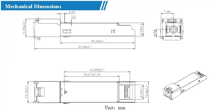
Mechanical Dimensions
Please refer to the mechanical dimensions drawing (Unit: mm)
Ordering Information
| Part Number | Product Description |
|---|
| SPT-GT4321-SB2BD | Tx1490nm Rx1310nm 2.5Gbps/1.25Gbps Class B+ SC Interface, 0°C ~ +70°C, With DDM |
| SPT-GT4321-SC2AD | Tx1490nm Rx1310nm 2.5Gbps/1.25Gbps Class C+ SC Interface, 0°C ~ +70°C, With DDM |
| SPT-GT4321-SC2CD | Tx1490nm Rx1310nm 2.5Gbps/1.25Gbps Class C++ SC Interface, 0°C ~ +70°C, With DDM |
| SPT-GT4321-SC2DD | Tx1490nm Rx1310nm 2.5Gbps/1.25Gbps Class C+++ SC Interface, 0°C ~ +70°C, With DDM |
| SPT-GT4321-SC2ED | Tx1490nm Rx1310nm 2.5Gbps/1.25Gbps Class C++++ SC Interface, 0°C ~ +70°C, With DDM |
Contact Us
Email: info@sopto.com.cn
Web: http://www.sopto.com.cn
Note: If you need more customized services, please contact us.